70MHz
70MHz transverter project
I've come up with the idea to build a 70MHz transverter. However, most existing transverter designs have 28MHz as intermediate frequency (IF). But, since I don't own a HF transceiver, I want to build a transverter with a 145MHz IF.
Despite some discouraging warnings from some other amateurs who say that this is very difficult to do, due to the small difference between the LO (75MHz) and the 70MHz band, I still want to try it.
Jan 15, 2012: First experiments with preparing the 75MHz LO signal, from a 25MHZ XO block (dip 14).
I had a 25MHz XO block in the "junkbox" that I want to use as the basis for the 75MHz LO. This was salvaged from an old PC, so the output is a TTL square-wave. Perfect, since the 3rd harmonic (75Mhz) is very strong (and so are 5th, 7th, 9th and so forth).
Following the 25MHz XO, a bandpass filter (double LC-parallel resonator), (tuned to 75MHz) will select the desired LO-frequency from a the harmonics.
Next, a MMIC buffer amplifier (MAR-1SM or perhaps MSA08-89) followed by another bandpass filter will hopefully result in a nice clean 75Mhz LO signal of suitable level (0dBm at least).
The schematic diagram of the LO chain (version 1):
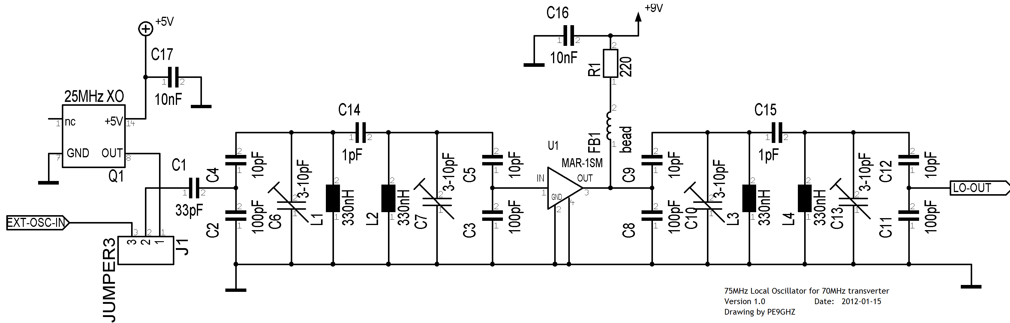
(click to view larger schematic in a new window)
The Receive (RX) converter will be based on a NE602/612, preceded by a double (LC-parallel) bandpass preselector and a pre-amp.
The Transmit (TX) mixer will be based on a IAM81008 (MMIC Active Double Balanced
Mixer/IFAmp), some bandpass filters and MMIC amplifiers.
Jan 15, 2012: Today I started the design of the PCB artwork for above described 75MHz LO. Here is version 1:
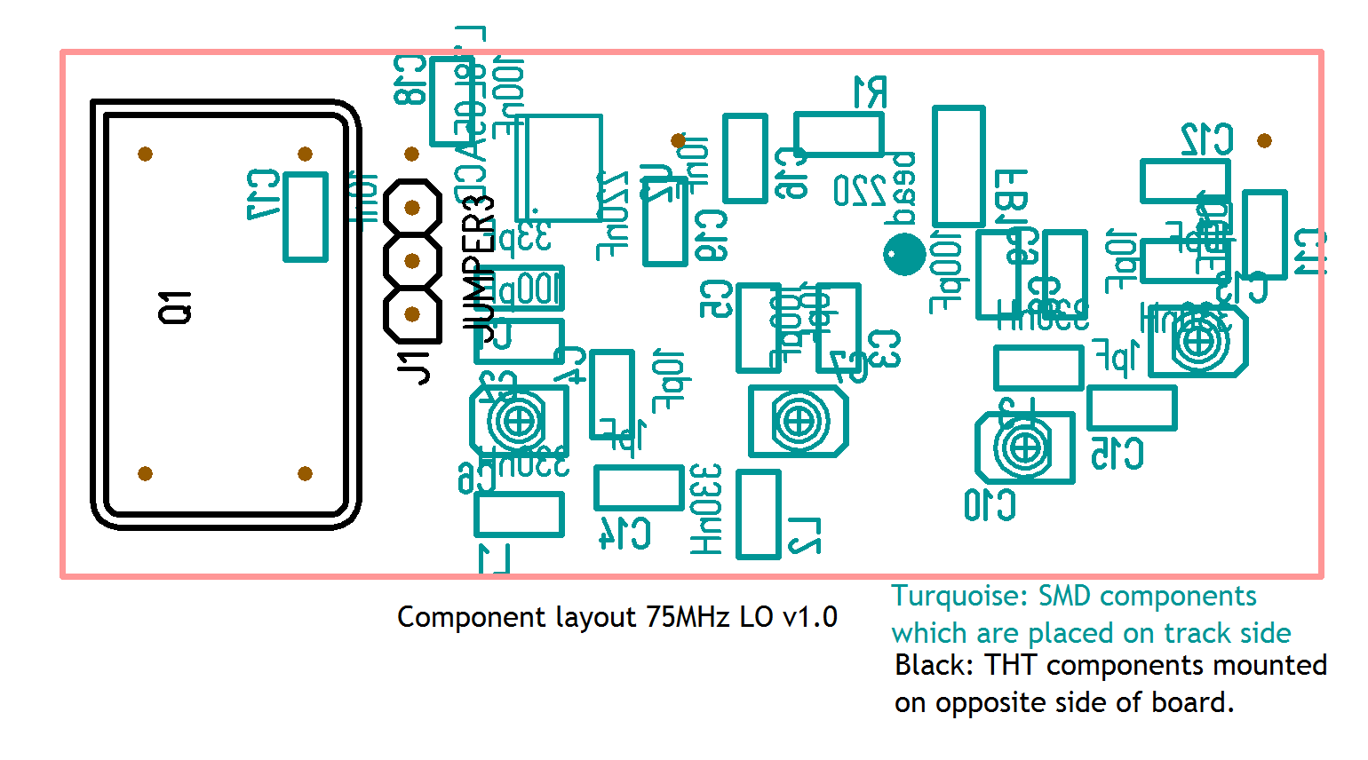
PCB Artwork:
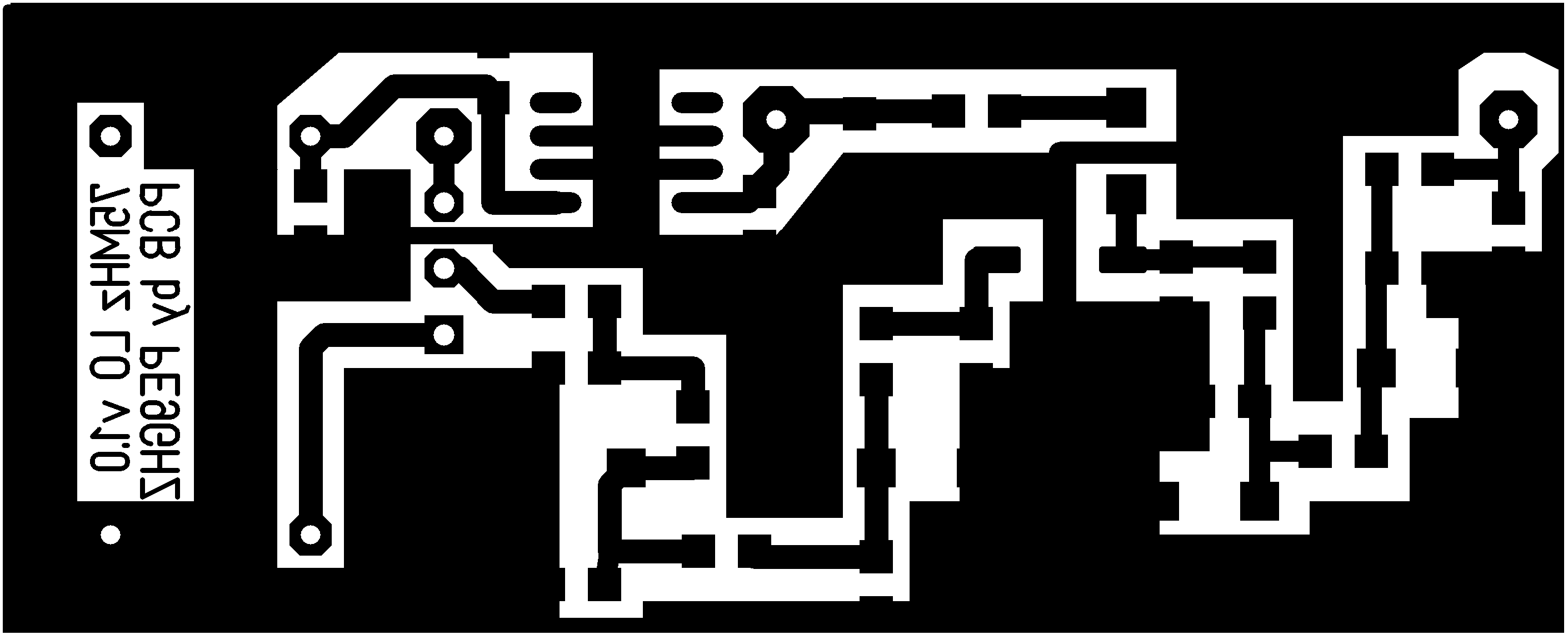
Actual board size: 60x25mm. It uses SMT / SMD resistors, inductors and capacitors of size 0805
Material: Double cladded FR4 1,5mm. Top side: all copper ground plane, except where holes for THT components are.
A 78L05A (SOIC8) regulator is included on the PCB to supply 5V to the XO block. This also ensures a good decoupling of 25MHz bleedthrough on the supply rail.
The board has yet to be etched, drilled and the components mounted.
Jan 19, 2012: In the past couple of days, I etched, drilled and assembled the 75MHz LO. Tonight, I did the alignment and some measurements. The fundamental frequency (25MHz) was not measurable with my spectrum analyser, and so was the 2nd harmonic (50MHz). LO-output @ 75MHz had a level of -2dBm. Higher harmonics were all down -60dBc or better.
I'd expected the 75MHz signal to be at a somewhat higher output level. -2dBm is probably not enough (after dividing it into 2 equal LO signals for Rx and Tx they'll be at -5 to -6dBm each). The NE612 requires 200-300mVtt (roughly -4dBm to -0,45dBm in 50Ohm), whereas just -5dBm suffices for the IAM81002 mixer. When using a resistive hybrid power splitter (-6dB each leg) we need an LO power of +2 to +5dBm).
So in the next few days I'll do some optimising on the output bandpass filter circuits (around C9-L3 / C12-L4), trying to bring down the insertion loss: I've measured the power level at the MAR-1SM output and it was at around +6dBm (more then sufficient), so the bandpass filter has an insertion loss of 8dB, which is quite high. Perhaps increasing the coupling cap C15 from 1pF to 2p2 or so will lower the insertion loss. I've also noticed that some of the trimmer caps are now set at their maximum capacity, so maybe these L/C circuits are not exactly tuned to 75MHz.
To be continued....
Jan 21, 2012: Increasing C15 to 2p2 (or even 3p3) did not result in more output (even less!), so I tried some other changes to the circuit: Change C8 and C11 from 100pF to 82pF resulted in a raise of 2dB. I'll experiment a bit more with the values of C8 and C11 to find the optimum..
Page modified by Eddy on 2012-01-22
Previous page: 1,3+ 5,7 + 10 + 24GHz Personal Beacons PE9GHZ/B
Next page: AD9835 DDS